In the Next 20 Years, Samsung Plans to Invest 230 Billion US Dollars in Chip Manufacturing
South Korean tech giant Samsung Electronics is expected to invest $230 billion over the next 20 years to develop what the country's government says is the world's largest chip manufacturing base, in line with efforts to boost the nation's chip industry.

As one of the largest electronics companies in South Korea,Samsung has been a major player in the semiconductor industry and is one of the largest semiconductor manufacturers in the world. In recent years, Samsung has invested heavily in expanding its semiconductor business, particularly in the production of advanced chips for applications such as artificial intelligence, 5G, and the internet of things. Samsung has also announced plans to invest heavily in research and development in these areas to stay at the forefront of technological innovation.
Samsung Electronics plans to build five fabs.Samsung is the world's largest maker of memory chips, smartphones and televisions. Under the official plan, companies in the high-tech sector will receive incentives such as expanded tax breaks and infrastructure support.
Paul Triolo, of global consultancy Albright Stonebridge Group, told the BBC that South Korea's move comes as "major players are stepping up efforts to move the semiconductor industry closer to Shore Manufacturing".
Semiconductors, which power everything from cellphones to military hardware, are at the heart of bitter disputes between the United States and various countries. Last week, the Netherlands said it also planned to restrict exports of its "state-of-the-art" microchip technology to protect national security. Around the same time, South Korea’s trade ministry raised concerns about U.S. semiconductor policy.

In addition to the huge investment, Samsung Electronics hired Lin Juncheng, a former senior engineer of TSMC, as the vice president of the advanced packaging business team of the semiconductor (DS) department. Vice President Lin will carry out the development of advanced 3D packaging technology in the organization in the future. In addition, Samsung Electronics' wafer foundry department poached Lee Sang-hoon, vice president of research on advanced lithography process extreme ultraviolet technology, from Intel.
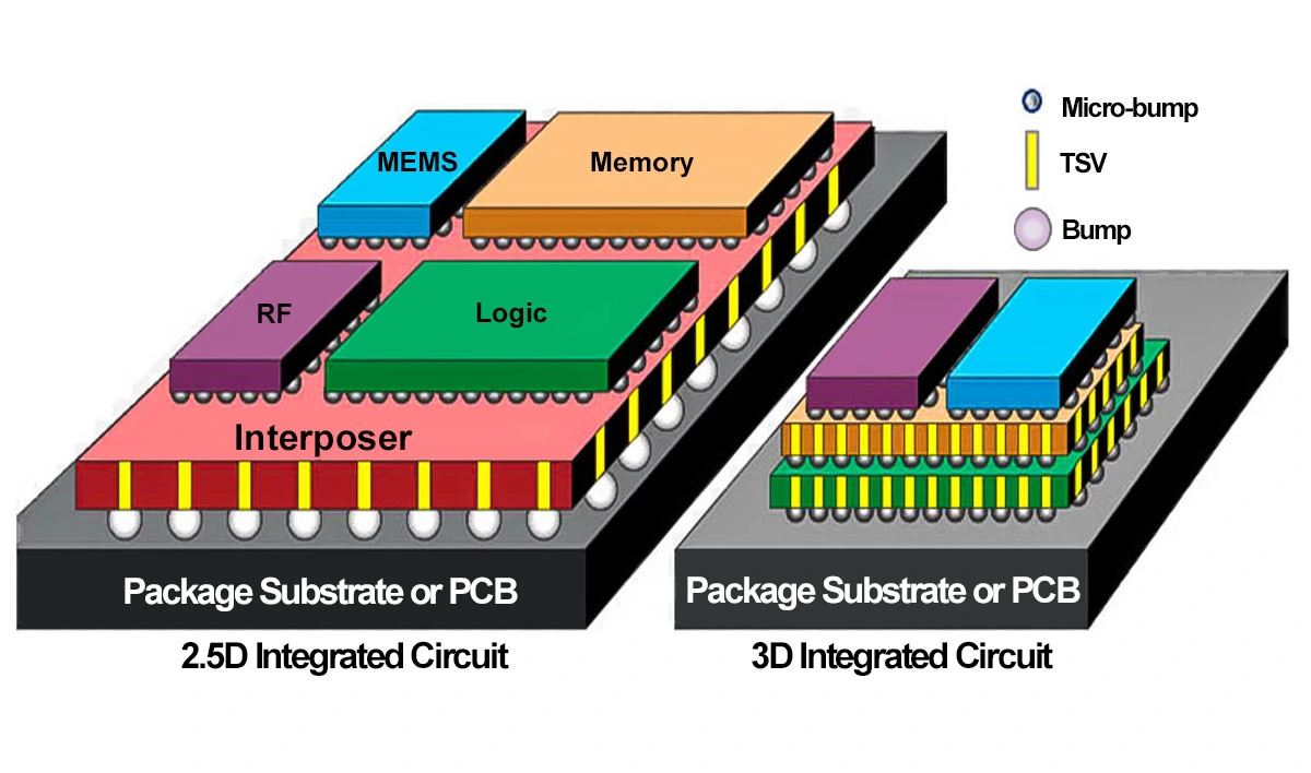
As front-end nodes get smaller, design cost becomes more important. Advanced Packaging (AP) solutions help address these issues by reducing cost, improving system performance, reducing latency, increasing bandwidth, and power efficiency.
High-end performance package platforms are UHD FO, Embedded Si Bridge, Si Interposer, 3D Stacked Memory and 3DSoC. There are two solutions for embedded silicon bridges: TSMC's LSI and Intel's EMIB. For Si interposers, there are usually classic versions from TSMC, Samsung, and UMC, as well as Intel's Foveros. EMIB combined with Foveros resulted in Co-EMIB for Intel's Ponte Vecchio. Meanwhile, 3D stack memory is represented by three categories of HBM, 3DS, and 3D NAND stack.
Intel is the industry's largest investor, noting $3.5 billion. Its 3D chip stacking technology is Foveros, which involves stacking chips on an active silicon interposer. The embedded multi-die interconnect bridge is its 2.5D packaging solution with 55-micron bump pitch. The combination of Foveros and EMIB gave birth to Co-EMIB for use in Ponte Vecchio GPUs.
Intel plans to use hybrid bonding technology for Foveros Direct. TSMC followed with $3.05 billion in capex. While capturing more business for UHD FO with InFO solutions, TSMC is also defining new system-level roadmaps and technologies for 3D SoCs.
Its CoWoS platform offers RDL or silicon interposer solutions, while its LSI platform is a direct competitor to EMIB. TSMC has become a high-end packaging giant with a leading front-end advanced node that can dominate the next generation of system-in-package.
Samsung has I-Cube technology similar to CoWoS-S. Samsung is one of the leaders in 3D stack memory solutions, offering HBM and 3DS. Its X-Cubes will use hybrid bonding interconnects.
With an estimated $2 billion capex for advanced packaging, ASE is the largest and only OSAT trying to compete with foundries and IDMs for packaging activity. With its FoCoS offering, ASE is also currently the only OSAT with a UHD FO solution.
Other OSATs do not have the financial and front-end capabilities to keep pace with big players like Intel, TSMC, and Samsung in the advanced packaging race.


 Need Help?


